How do I troubleshoot the ESP32 USB JTAGUART interface on a new PCB Circuit Diagram All projects are explained with step-by-step instructions with the components list, circuit diagram, source code, and all other required resources and information you need to build those ESP32 projects. You can also explore projects with different IoT platforms like ESP RainMaker, IFTTT, Blynk IoT. Amazon Alexa, Google Home, Arduino IoT Cloud, etc. 1.5 Block Diagram 5 2 Pin Definitions 6 2.1 Pin Layout 6 2.2 Pin Description 6 2.3 Power Scheme 8 2.4 Strapping Pins 9 3 Functional Description 10 3.1 CPU and Memory 10 As such, the entire solution occupies minimal Printed Circuit Board (PCB) area. ESP32 uses CMOS for single-chip fully-integrated radio and baseband, and also integrates
You signed in with another tab or window. Reload to refresh your session. You signed out in another tab or window. Reload to refresh your session. You switched accounts on another tab or window. ESP32 is a tiny cheap 8$ module with a dual core 32-bit CPU and built in Wi-Fi and dual-mode Bluetooth with sufficient amount of 30 I/O pins for all basic electronics projects.All these features are very easy to use, since it can be programmed directly from the Arduino IDE. Explore below the list of ESP32 projects to start with ESP32 based IoT projects.
ESP32 Projects with Code and Circuit Diagram
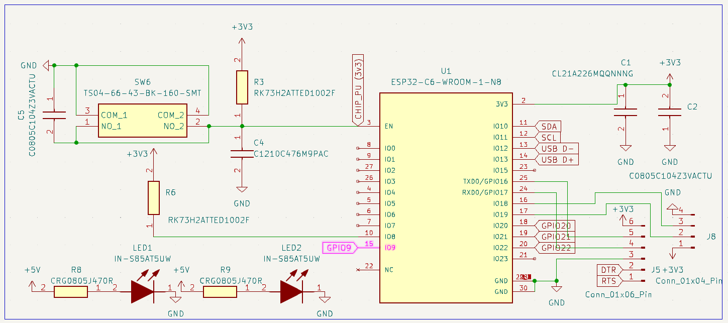
The high integration of ESP32-S3 allows for simple peripheral circuit design. This chapter details the schematic design of ESP32-S3. The following figure shows a reference schematic design of ESP32-S3. It can be used as the basis of your schematic design. ESP Hardware Design Guidelines . This document provides guidelines for the ESP32 SoC.To switch to another chip, use the drop-down menu at the top left of the page.

Figure ESP32 RF Tuning Diagram shows the general process of RF tuning. Figure ESP32 Schematic for External Capacitor shows the schematic of components connected to pin47 CAP2 and pin48 CAP1. C5 (10 nF) that connects to CAP1 should be of 10% tolerance and is required for proper operation of ESP32. In conclusion, reading and interpreting the Esp32 schematic diagram is a crucial skill for understanding the design and functionality of the board. By identifying key components, understanding connections, recognizing symbols, and referring to the datasheet, you can gain a comprehensive understanding of the Esp32 schematic diagram. Learn about the ESP32 microcontroller, its features, and how to use it with various development boards. Find the pinout, specifications, datasheet, and schematic of ESP32 WROOM-32 chip and ESP32 boards.
